2�
� RF Device Data�
� Freescale Semiconductor�
� MRF7S21150HR3 MRF7S21150HSR3�
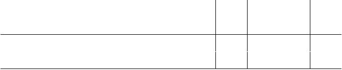
� Table 3. ESD Protection Characteristics�
� Test Methodology�
� Class�
� Human Body Model (per JESD22-A114)�
� 1C (Minimum)�
� Machine Model (per EIA/JESD22-A115)�
� A (Minimum)�
� Charge Device Model (per JESD22-C101)�
� IV (Minimum)�
� Table 4. Electrical Characteristics (TC�
� = 25�
� °C unless otherwise noted)�
� Characteristic�
� Symbol�
� Min�
� Typ�
� Max�
� Unit�
� Off Characteristics�
� Zero Gate Voltage Drain Leakage Current�
� (VDS�
� = 65 Vdc, V�
� GS�
� = 0 Vdc)�
� IDSS�
� ?�
� ?�
� 10�
� μAdc�
� Zero Gate Voltage Drain Leakage Current�
� (VDS�
� = 28 Vdc, V�
� GS�
� = 0 Vdc)�
� IDSS�
� ?�
� ?�
� 1�
� μAdc�
� Gate-Source Leakage Current�
� (VGS�
� = 5 Vdc, V�
� DS�
� = 0 Vdc)�
� IGSS�
� ?�
� ?�
� 1�
� μAdc�
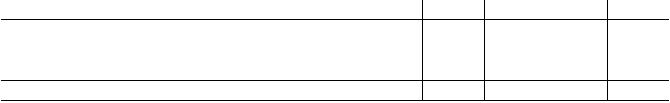
� On Characteristics�
� Gate Threshold Voltage�
� (VDS�
� = 10 Vdc, I�
� D�
� = 348 �
� μAdc)�
� VGS(th)�
� 1.2�
� 2�
� 2.7�
� Vdc�
� Gate Quiescent Voltage�
� (VDS�
� = 28 Vdc, I�
� D�
� = 1350 mAdc)�
� VGS(Q)�
� ?�
� 2.7�
� ?�
� Vdc�
� Fixture Gate Quiescent Voltage�
� (1)�
� (VDD�
� = 28 Vdc, I�
� D�
� = 1350 mAdc, Measured in Functional Test)�
� VGG(Q)�
� 4.5�
� 5.4�
� 6.5�
� Vdc�
� Drain-Source On-Voltage�
� (VGS�
� = 10 Vdc, I�
� D�
� = 2.7 Adc)�
� VDS(on)�
� 0.1�
� 0.15�
� 0.3�
� Vdc�
� Dynamic Characteristics (2)�
� Reverse Transfer Capacitance�
� (VDS�
� = 28 Vdc �
� ±�
� 30 mV(rms)ac @ 1 MHz, V�
� GS�
� = 0 Vdc)�
� Crss�
� ?�
� 0.9�
� ?�
� pF�
� Output Capacitance�
� (VDS�
� = 28 Vdc �
� ±�
� 30 mV(rms)ac @ 1 MHz, V�
� GS�
� = 0 Vdc)�
� Coss�
� ?�
� 590�
� ?�
� pF�
� Input Capacitance�
� (VDS�
� = 28 Vdc, V�
� GS�
� = 0 Vdc �
� ±�
� 30 mV(rms)ac @ 1 MHz)�
� Ciss�
� ?�
� 320�
� ?�
� pF�
� Functional Tests�
� (In Freescale Test Fixture, 50 ohm system) V�
� DD�
� = 28 Vdc, I�
� DQ�
� = 1350 mA, P�
� out�
� = 44 W Avg., f = 2112.5 MHz and�
� f = 2167.5 MHz, Single-Carrier W-CDMA, IQ Magnitude Clipping, PAR = 7.5 dB @ 0.01% Probability on CCDF. ACPR measured in�
� 3.84 MHz Channel Bandwidth @ ±5 MHz Offset.�
� Power Gain�
� Gps�
� 16.5�
� 17.5�
� 19.5�
� dB�
� Drain Efficiency�
� ηD�
� 29�
� 31�
� ?�
� %�
� Output Peak-to-Average Ratio @ 0.01% Probability on CCDF�
� PAR�
� 5.7�
� 6.1�
� ?�
� dB�
� Adjacent Channel Power Ratio�
� ACPR�
� ?�
� -37�
� -35�
� dBc�
� Input Return Loss�
� IRL�
� ?�
� -15�
� -9�
� dB�
� 1. VGG�
� = 2 x V�
� GS(Q). Parameter measured on Freescale Test Fixture, due to resistive divider network on the board. Refer to Test Circuit�
� schematic.�
� 2. Part internally matched both on input and output.�
� (continued)�
�  �
�
� � �  �
�
� � �  �
�
� � �  �
�
� � �  �
�
� � �  �
�
� � �  �
�
� � �  �
�
� � 发布紧急采购,3分钟左右您将得到回复。
相关PDF资料
MRF7S21170HR5
IC MOSFET RF N-CHAN NI-880
MRF7S21210HSR5
MOSFET RF N-CH 63W NI-780S
MRF7S27130HSR5
MOSFET RF N-CH 23W NI-780S
MRF7S35015HSR5
MOSFET RF N-CH 15W NI-400S-240
MRF7S35120HSR5
MOSFET RF N-CH 120W NI-780S
MRF7S38010HSR5
MOSFET RF N-CH 2W 30V NI-400S
MRF7S38040HSR5
MOSFET RF N-CH 8W 30V NI-400S
MRF7S38075HSR5
MOSFET RF N-CH 12W 30V NI-780S
相关代理商/技术参数
MRF7S21170HR3
功能描述:射频MOSFET电源晶体管 HV7 2.1GHZ WCDMA NI880H RoHS:否 制造商:Freescale Semiconductor 配置:Single 晶体管极性: 频率:1800 MHz to 2000 MHz 增益:27 dB 输出功率:100 W 汲极/源极击穿电压: 漏极连续电流: 闸/源击穿电压: 最大工作温度: 封装 / 箱体:NI-780-4 封装:Tray
MRF7S21170HR3_07
制造商:FREESCALE 制造商全称:Freescale Semiconductor, Inc 功能描述:RF Power Field Effect Transistors N-Channel Enhancement-Mode Lateral MOSFETs
MRF7S21170HR3_08
制造商:FREESCALE 制造商全称:Freescale Semiconductor, Inc 功能描述:RF Power Field Effect Transistors
MRF7S21170HR3_11
制造商:FREESCALE 制造商全称:Freescale Semiconductor, Inc 功能描述:RF Power Field Effect Transistors N--Channel Enhancement--Mode Lateral MOSFETs
MRF7S21170HR3_12
制造商:FREESCALE 制造商全称:Freescale Semiconductor, Inc 功能描述:RF Power Field Effect Transistors
MRF7S21170HR5
功能描述:射频MOSFET电源晶体管 HV7 2.1GHZ WCDMA NI880H RoHS:否 制造商:Freescale Semiconductor 配置:Single 晶体管极性: 频率:1800 MHz to 2000 MHz 增益:27 dB 输出功率:100 W 汲极/源极击穿电压: 漏极连续电流: 闸/源击穿电压: 最大工作温度: 封装 / 箱体:NI-780-4 封装:Tray
MRF7S21170HS
功能描述:IC MOSFET RF N-CHAN NI-880S RoHS:是 类别:分离式半导体产品 >> RF FET 系列:- 产品目录绘图:MOSFET SOT-23-3 Pkg 标准包装:3,000 系列:- 晶体管类型:N 通道 JFET 频率:- 增益:- 电压 - 测试:- 额定电流:30mA 噪音数据:- 电流 - 测试:- 功率 - 输出:- 电压 - 额定:25V 封装/外壳:TO-236-3,SC-59,SOT-23-3 供应商设备封装:SOT-23-3(TO-236) 包装:带卷 (TR) 产品目录页面:1558 (CN2011-ZH PDF) 其它名称:MMBFJ309LT1GOSMMBFJ309LT1GOS-NDMMBFJ309LT1GOSTR
MRF7S21170HSR3
功能描述:射频MOSFET电源晶体管 2.1GHZ HV7 WCDMA NI880HS RoHS:否 制造商:Freescale Semiconductor 配置:Single 晶体管极性: 频率:1800 MHz to 2000 MHz 增益:27 dB 输出功率:100 W 汲极/源极击穿电压: 漏极连续电流: 闸/源击穿电压: 最大工作温度: 封装 / 箱体:NI-780-4 封装:Tray